FPGA Capacitive Keyboard Synthesizer
An FPGA-Based Musical Instrument With Custom Capacitive Sensing and Digital Audio Synthesis
WHY — Motivation, Problem, and Constraints
The FPGA Capacitive Synthesizer was my final project for Digital Systems Laboratory (6.205), developed in collaboration with Adan Abu Naaj.
The motivation behind the project was to explore how capacitive sensing can enable a level of expressiveness in electronic musical instruments that is difficult to achieve with traditional buttons, keys, or potentiometers. Conventional digital synth interfaces tend to discretize interaction—notes are on or off, parameters jump between values—which limits the user's ability to make fluid, continuous gestures.
Capacitive interfaces, by contrast, naturally support continuous, gesture-based control. A performer can smoothly slide across pitches, modulate parameters in real time with finger position or pressure, and control multiple dimensions of sound simultaneously. For example, a vertical column of ribbon-shaped capacitive pads can be mapped to a single note, allowing per-note control over filters or effects while the note is held—something that is cumbersome or impossible with standard key-based interfaces.
Achieving this level of expressiveness requires scanning many capacitive sensors at high rates and mapping them to sound parameters with minimal latency. An FPGA is well-suited to this problem: it allows massively parallel sensor scanning, deterministic timing, and low-latency signal processing that would be difficult to guarantee on a microcontroller or general-purpose CPU.
The project was inspired by expressive touchscreen-based instruments such as GeoShred, with the goal of implementing similar expressive capabilities in a custom hardware instrument built around capacitive sensing and FPGA-based real-time control.
Project Constraints
Hardware Specs
- Spartan-7 FPGA
- Limited BRAM + DSP slices
Performance
- Touch → Audio latency < 10ms
- Instantaneous feel
Complexity
- Polyphonic mixing w/ arbitration
- No off-the-shelf IP cores
Sensing
- 24–36 capacitive pads
- Noisy & timing-sensitive
WHAT — System Overview
A high-level architecture view:
Hardware System Components
Capacitive Interface (My Work)
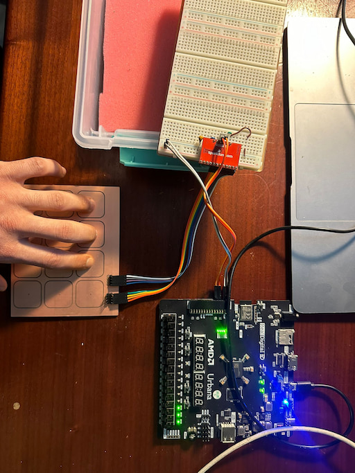
Iteration 1: Proof of Concept
The first iteration (below) was a simple 4x3 grid used to validate our custom I2C drivers and touch sensitivity.
Iteration 2: Final Design
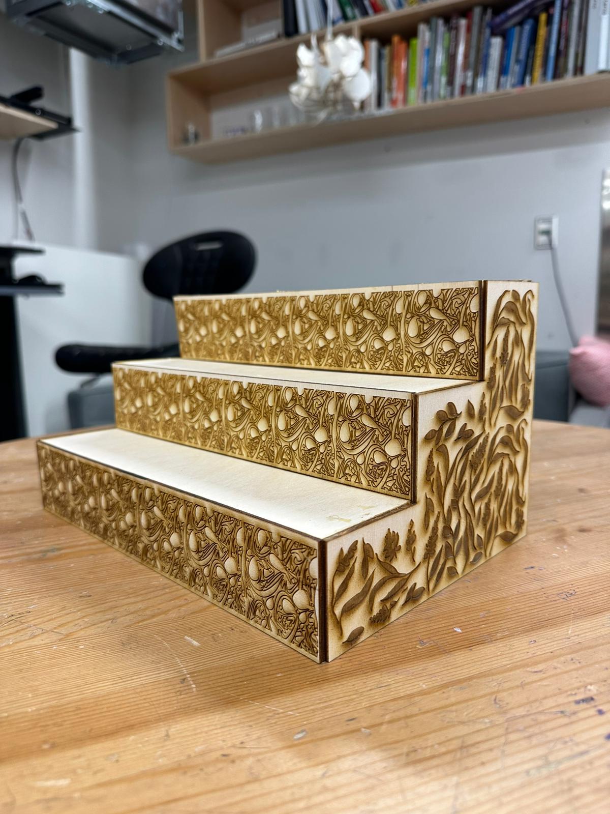
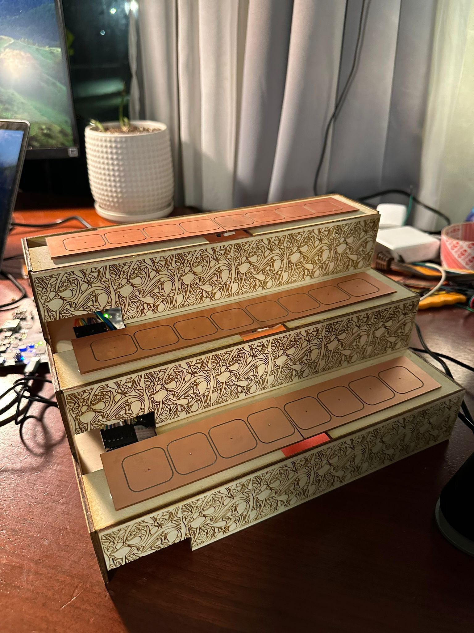
The final interface (below) consists of three separate rows of 8 capacitive pads each, designed to align perfectly with the laser-cut body.
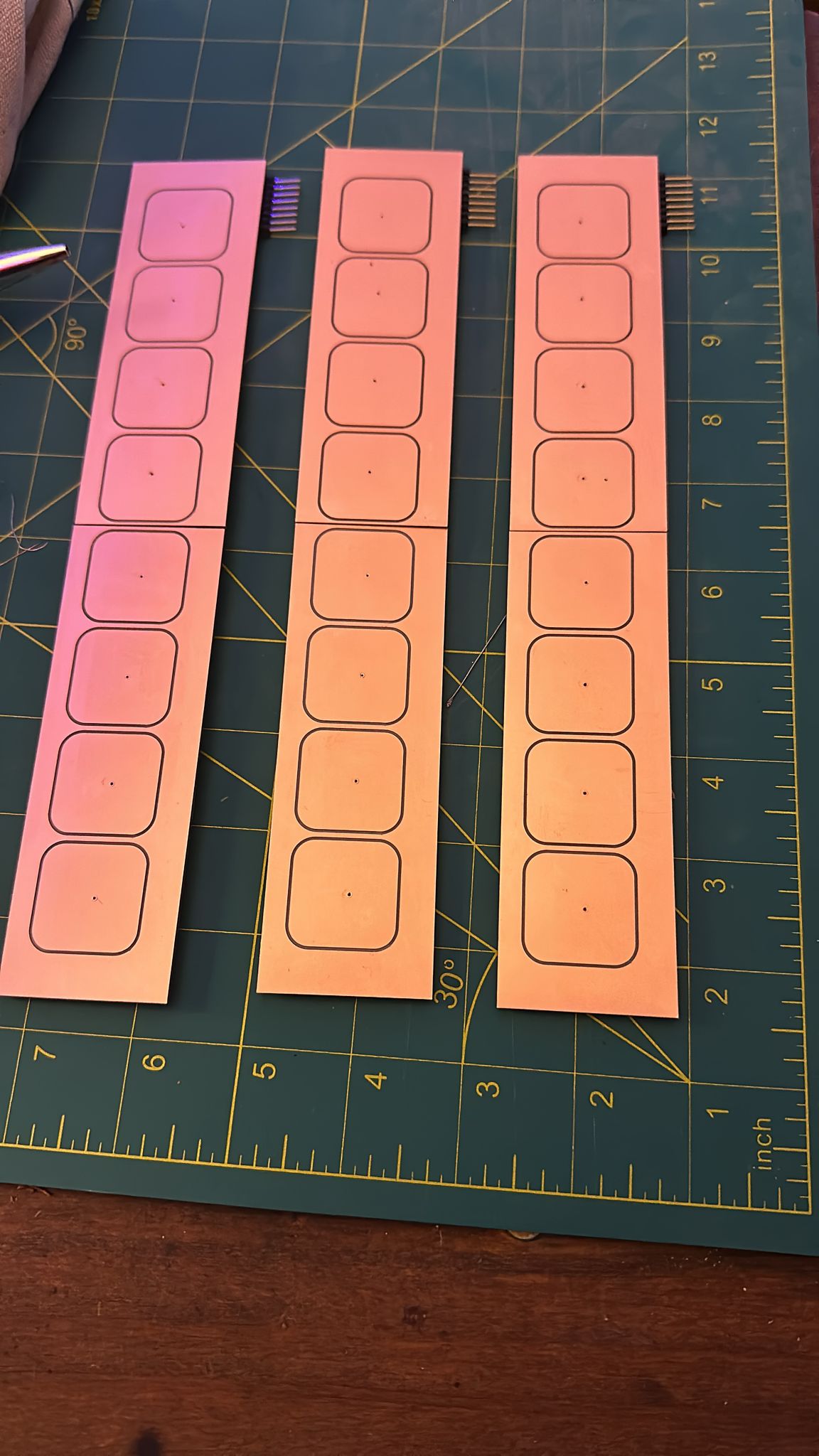
Fabrication Constraint: We milled the PCBs on an Othermill, which has a max bed width of 140mm—too short for a full 8-pad strip.
Solution: Each 8-pad row is actually composed of two 4-pad PCBs joined on the underside with SMD horizontal headers.
- 24 copper pads total
- 3× MPR121 ICs
- Address-configured to scale to 36+ pads
- Routed via PMOD cables to FPGA board
Custom I²C Controller (My Work)
High-Stakes Hardware Debugging
Unlike authentic Adafruit boards, the knockoff MPR121 modules we sourced had a manufacturing defect where the address selection pin was hardwired to 0x5A, making multi-chip communication impossible. To fix this, I had to reverse-engineer the PCB trace and physically cut the hidden connection with an X-Acto knife to restore address configurability.
To achieve low-latency multi-chip polling, I designed a hand-written 10-state I²C finite-state machine rather than relying on a microcontroller bridge. This gave me direct control over bus timing, repeated-start sequencing, and bounded retry behavior.
Key Challenges & Solutions
- Bidirectional SDA: Implemented precise state-driven enable/disable logic to handle the bidirectional data line without contention.
- Metastability Protection: All incoming SDA/SCL signals pass through dual-flop synchronizers.
- Recovery Path: On a missing ACK, the FSM issues a STOP condition, waits the required bus-free interval, and retries the transaction up to a fixed limit.
- Repeated Start: The FSM explicitly handles the repeated-start sequence needed to read MPR121 registers without releasing the bus.
Below is the core state transition logic:
typedef enum logic [3:0] {
  IDLE, START, ADDR, AWAIT_ACK, READ_ACK,
  PROCESS_ACK, DATA, READ, STOP, BUS_FREE_TIME
} state_t;


// ...


IDLE: begin
        scl_toggle_en <= 1'b0;
        scl_overdrive <= 1'b1;
        sda_val <= 1'b1;
        data_valid_out <= 1'b0;
        ack_out <= 1'b0;
        if (start) begin
          state <= START;
        end
      end
      START: begin

        ack_out <= 1'b0;
        if (prev_byte == CMD_BYTE) begin
          //repeated start
          peripheral_addr_in_reg[0] <= 1'b1;
        end else begin
          peripheral_addr_in_reg <= {peripheral_addr_in, 1'b0};
          rw_reg <= rw;
          data_byte_in_reg <= data_byte_in;
          command_byte_in_reg <= command_byte_in;
          ack_out <= 1'b0;
        end
        scl_toggle_en <= 1'b1;
        sda_val <= 1'b0;
        bit_count <= 7;
        state <= ADDR;


      end
      ADDR: begin
        //wait for first scl toggle to 0, then start sending data on falling edge.
        //each bit of data stays on the line as long as scl is high
        if (scl_falling_edge) begin
          sda_val <= peripheral_addr_in_reg[bit_count];
          if (bit_count == 0) begin
            state <= AWAIT_ACK;
            prev_byte <= ADDR_BYTE;
          end else begin
            bit_count <= bit_count - 1;
          end
        end
      end
      AWAIT_ACK: begin
        //maintain sda upto next falling edge. then set to high impedence to read sda.
        if (scl_falling_edge) begin
          sda_val <= 1'b1;//sets sda_out to high impedence
          state <= READ_ACK;
        end
      end
      READ_ACK: begin
        //wait for scl to go high, then read sda over the clock cycles in the middle of the high period
        if (half_period_count == QUARTER_PERIOD && scl_out) begin
          ack_in <= sda;
          state <= PROCESS_ACK;
        end
      end
      PROCESS_ACK: begin
        if ((prev_byte == DATA_BYTE) && peripheral_addr_in_reg[0]) begin
          //read; end repeated start with a NACK. just need to keep sda high
          state <= STOP;
        end else begin
          if (!ack_in)begin
            //ack recieved
            if (rw_reg) begin
              if (prev_byte == CMD_BYTE) begin
                //read; repeated start
                if(scl_rising_edge) begin
                  state <= START;
                end

              end else if (peripheral_addr_in_reg[0]) begin
                state <= READ;
                sda_val <= 1'b1; // set to high impedence to read sda
              end else begin
                state <= DATA;
              end
              bit_count <= 7;
            end else begin
              if (prev_byte == DATA_BYTE) begin
                state <= STOP;
              end else begin
                state <= DATA;
                bit_count <= 7;
              end
            end
          end else begin
            //no ack recieved
            state <= STOP;
            retry_count <= retry_count + 1;
            ack_out <= 1'b1;
          end
        end
      end
      DATA: begin
        if (prev_byte == ADDR_BYTE) begin
          //command byte follows if write. data byte follows if read in repeated start phase(indicated by the rw bit of the addr byte)
          if (scl_falling_edge) begin
            sda_val <= command_byte_in_reg[bit_count];
            if (bit_count == 0) begin
              state <= AWAIT_ACK;
              prev_byte <= CMD_BYTE;
            end else begin
              bit_count <= bit_count - 1;
            end
          end
        end else if (prev_byte == CMD_BYTE) begin
          //data byte follows
          if (scl_falling_edge) begin
            sda_val <= data_byte_in_reg[bit_count];
            if (bit_count == 0) begin
              state <= AWAIT_ACK;
              prev_byte <= DATA_BYTE;
            end else begin
              bit_count <= bit_count - 1;
            end
          end
        end
      end
      READ: begin
        if (scl_rising_edge) begin
          data_byte_out[bit_count] <= sda;
          if (bit_count == 0) begin
            state <= AWAIT_ACK;
            prev_byte <= DATA_BYTE;
          end else begin
            bit_count <= bit_count - 1;
          end
        end
      end
      STOP: begin
        //ENSURE TBUF IS NOT VIOLATED
        //need 0.6 ms delay before sda is pulled back high. add delay of 60 cycles between scl rising and sda rising
        if (!scl_toggle_en) begin
          if (stop_setup_count == STOP_SETUP_CYCLES) begin
            sda_val <= 1'b1;
            state <= BUS_FREE_TIME;
            prev_byte <= STOP_BYTE;
            stop_setup_count <= 0;
          end else begin
            stop_setup_count <= stop_setup_count + 1;
          end
        end else if (scl_falling_edge) begin
          sda_val <= 1'b0;
        end else if (scl_rising_edge) begin
          scl_toggle_en <= 1'b0;
          stop_setup_count <= 0;
        end
      end
      BUS_FREE_TIME: begin
        //wait for 1.3 ms before next start condition
        if (stop_setup_count == BUS_FREE_CYCLES) begin
          if (!ack_out) begin
            data_valid_out <= 1'b1;
            state <= IDLE;
            retry_count <= 0;
          end else begin
            //retry
            if (retry_count == 4'd10) begin
              state <= IDLE;
              retry_count <= 0;
              ack_out <= 1'b0;
            end else begin
              state <= START;
              retry_count <= retry_count + 1;
            end
          end
          stop_setup_count <= 0;
        end else begin
          stop_setup_count <= stop_setup_count + 1;

        end
      end

    endcase
  // ...
This custom driver polls the MPR121 electrode-status registers (0x00–0x01) and exposes a clean 24-bit touch vector to the rest of the system.
This custom driver polls the MPR121 electrode-status registers (0x00–0x01) and exposes a clean 24-bit touch vector to the rest of the system.
.png)
I2C Read Format
.png)
I2C Write Format
MPR121 Driver Module(My Work)
Implements:
- Runtime configuration of thresholds
- Continuous electrode polling
- Combined 24-bit touch vector output
- Integration with interrupt-based updates
Note Decoder & Voice Allocation (My Work)
To keep the system modular, I separated gesture detection (touch processing) from voice triggering (synthesis).
- Input: 24-bit touch vector from I2C driver.
- Logic: Decodes raw capacitance into "Note On/Off" events.
- Output: Gate signals sent to the Polyphony Manager.
Digital Audio Synthesis
Two parallel sound-generation pipelines were implemented to compare synthesis techniques:
A. Procedural Synthesis (My Work)
The primary engine used Direct Digital Synthesis (DDS) with a 32-bit Phase Accumulator.
- Precision: 32-bit accumulator running at master clock allows extremely fine pitch control (smooth sliding).
- Formula:
phase_increment = (frequency * 2^32) / Fs - Waveforms: Top bits address a BRAM Look-Up Table (LUT) for Sine, Sawtooth, or Square waves.
B. Oud Sample Playback (Adan's Work)
To mimic a real Oud, we implemented a sample-based pipeline.
- Workflow: Recorded Audio → Python (Librosa) for trimming/normalization → 16kHz Downsampling →
.memfiles. - BRAM Layout: Used 4 cascaded BRAM blocks per note to store ~8k samples.
Design Pivot
While the sample playback worked, we found that improving realism became a software problem (better Python preprocessing) rather than a hardware problem. To maximize our FPGA learning outcomes, we deprioritized the sampler in the final build and focused on enhancing the Procedural Synthesis engine's real-time modulation features.
ADSR (Adan's Work)
- FSMD structure
- Attack → Decay → Sustain → Release
- Smooth multiplier applied to waveform sample
- One ADSR per voice → enables polyphony
Polyphony Architecture & Mixing (Shared Work)
The system supports 8 simultaneous voices. Managing this on a Spartan-7 required careful resource sharing:
- Challenge: Summing 8 voices blindly would cause integer overflow and digital clipping.
- Solution: A Pipelined Summation Tree with Dynamic Normalization.
The mixer monitors the number of active voices and bit-shifts the output to maintain a constant volume level, whether 1 or 8 notes are playing. This avoids expensive division operations.
// Dynamic Normalization logic to prevent clipping
case(note_count)
    4'd1: multiplied_sum <= sum * 255; // Scale to maintain volume
    4'd2: multiplied_sum <= sum * 128; // ~ 1/2 gain
    4'd3: multiplied_sum <= sum * 85;  // ~ 1/3 gain
    // ...
    4'd8: multiplied_sum <= sum * 32;  // ~ 1/8 gain
    default: multiplied_sum <= 0;
endcase
PDM Output Stage (My Work)
We chose Pulse Density Modulation (PDM) over PWM for the final audio output.
- Why? PDM pushes quantization noise into higher frequencies (noise shaping), which are easily removed by a simple analog RC low-pass filter, resulting in much cleaner audio than PWM at the same clock capability.
I implemented a First-Order Delta-Sigma Modulator to generate the PDM signal:
// Accumulator for PDM modulation (Delta-Sigma approach)
logic [PDM_RESOLUTION_WIDTH:0] accumulator;
logic [PDM_RESOLUTION_WIDTH:0] pdm_res_minus_dc;
assign pdm_res_minus_dc = PDM_RESOLUTION - dc_in;

always_ff @(posedge clk_in or posedge rst_in) begin
  if (rst_in) begin
    accumulator <= 0;
    sig_out <= 0;
  end else begin
    if (|gate_in) begin
      // If error (accumulator) exceeds threshold, pulse high and subtract reduction
      if (accumulator >= pdm_res_minus_dc) begin
        sig_out <= 1;
        accumulator <= accumulator - pdm_res_minus_dc;
      end else begin
        // Otherwise, keep low and accumulate error
        sig_out <= 0;
        accumulator <= accumulator + dc_in;
      end
    end else begin
      sig_out <= 0;
    end
  end
end
Enclosure & Fabrication (Adan's Work)
The body was laser-cut from plywood, designed to hide all wiring while keeping the capacitive pads accessible for playing.